- 12-06-2026
- Computer Vision
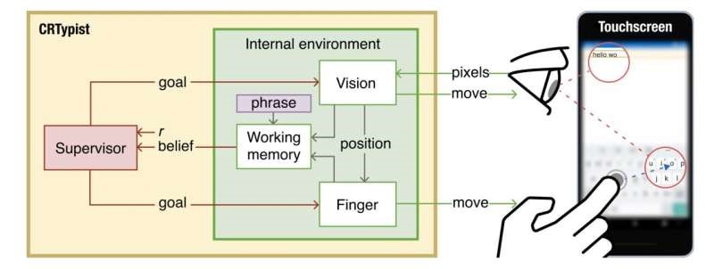
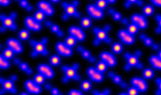
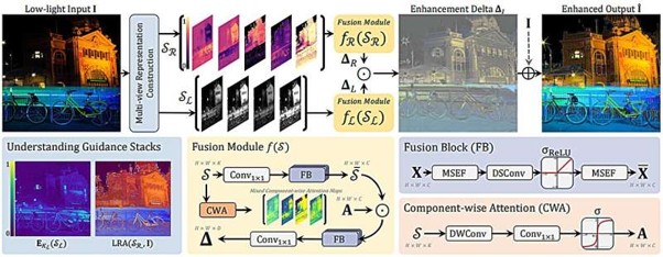
Researchers introduced Multinex, an ultra-lightweight AI model for low-light image enhancement that improves the clarity of dark and degraded images while maintaining high efficiency. Enabling real-time computer vision on edge devices.
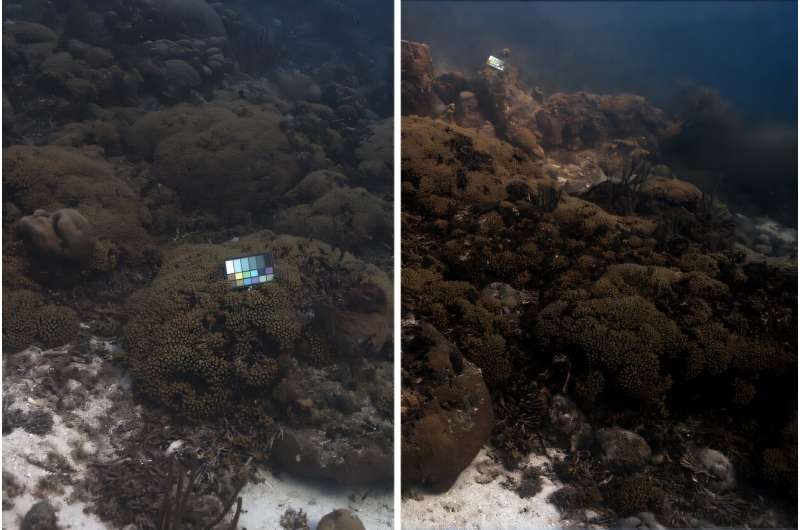
Low-light environments remain one of the biggest challenges for computer vision systems, often producing images with poor visibility, noise, and missing details. Multinex addresses this challenge through an efficient AI-based enhancement approach designed to restore image quality while keeping computational demands low.
Unlike larger deep learning models that require significant processing power, Multinex focuses on lightweight architecture, enabling faster and more efficient image improvement. This makes the technology particularly valuable for applications where resources are limited but visual accuracy is essential.
The advancement could benefit areas such as surveillance systems, autonomous technologies, mobile photography, robotics, and real-time monitoring solutions. By improving visibility in difficult lighting conditions, lightweight AI models like Multinex can help machines better understand their surroundings.
As artificial intelligence continues moving toward edge computing and real-world deployment, efficient models are becoming increasingly important. Multinex demonstrates how future AI systems can become smaller, faster, and more practical without sacrificing performance.